Multiple Choice Questions
Carbon, silicon and germanium atoms have four valence electrons each. Their valence and conduction bands are separated by energy band gaps represented by respectively. Which one of the following relationships is true in their case?
Choose the only false statement from the following
Substances with energy gap ofthe order of 10 eV are insulators
The conductivity of a semiconductor increases with increases in temperature
In conductors the valence and conduction bands may overlap
The resistivity of a semiconductor increases with increase in temperature
The total energy of an electron in the first excited state of hydrogen is about -3.4 eV. Its kinetic energy in this state is
-3.4 eV
-6.8 eV
6.8 eV
3.4 eV
The principle of LASER action involves
amplification of particular frequency emitted by the system
population inversion
stimulated emission
All of the above
Which of the following is unipolar transistor?
p-n-p transistor
n-p-n transistor
Field effect transistor
Point contact transistor
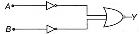
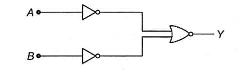
The truth table given below is for (A and B are the inputs, Y is the output)
| A | B | Y |
| 0 | 0 | 1 |
| 0 | 1 | 1 |
| 1 | 0 | 1 |
| 1 | 1 | 0 |
NOR
AND
XOR
NAND
The reason of current flow in p-n junction in forward bias is
drifting of charge carriers
drifting of minority charge carriers
diffussion of charge carriers
All of the above
A change of 8.0 mA in the emitter current brings a change of 7. 9 mA in the collector current. The value of a will be
0.96
0.93
0.90
0.99