Multiple Choice Questions
A p-type semiconductor is formed by adding 1 indium atom in to a sample of silicon per 5x10⁻⁷ silicon atoms. If the density of atoms in the sample is 5×1028 atoms/metre3, the number of atoms accepted in per metre3 of silicon is
1.0 × 10¹³ atoms/cm3
2.5 × 10²⁰ atoms/cm3
2.5 × 1025 atoms/cm3
1.0 × 10¹⁵ atoms/cm3
The energy gap between the valence band and the conduction band for a material is 6 eV. The material is
an insulator
a metal
an intrinsic semiconductor
a superconductor
An AC signal of 50 Hz frequency is input of a full wave rectifier using two diodes. The output frequency after full wave rectification is
25 Hz
50 Hz
100 Hz
200 Hz
Avalanche breakdown in a p-n junction diode is due to
shift of fermi level
widening of forbidden gap
high impurity concentration
cummulative effect of conduction band electrons collision
If dopping in the P region is high, then N region
depletion layer will be more towards P
depletion layer will be more towards N
depletion layer will remain unchanged
None of the above
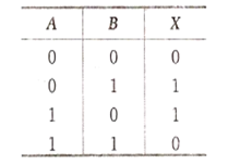
To get an output Y =1 from circuit of figure, the input must be
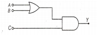
A = 0, B = 1, C = 0
A = 0, B = 0, C = 1
A = 1, B = 0, C = 0
A = 1, B = 0, C = 1