 Multiple Choice Questions
A p-n-p transistor is used in common-emitter mode in an amplifier circuit. A change of 45 µA in the base current brings a change of 3 mA in collector current and 0.05 V in base-emitter voltage. If a load of 7 kΩ is used, then voltage gain of amplifier is
729.25
824.41
236.34
424.27
A Zener diode, having breakdown voltage equal to 15 V, is used in a voltage regulator circuit shown in figure. The current through the diode is

5 mA
10 mA
15 mA
20 mA
In the following circuit, the output Y becomes one for the inputs
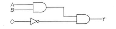
A= 0, B = 1, C = 0
A = 1, B = 1, C = 0
A =1, B= 1, C = 1
A = 1, B= 0, C = 1
Carbon, silicon and germanium atoms have four valence electrons each. Their valence and conduction bands are separated by energy band gaps represented by (Eg)C , (Eg )Si , and (Eg)Ge respectively. Which one of the following relationships is true in their case ?
(Eg)C > (Eg)Si
(Eg)C = (Eg)Si
(Eg)C < (Eg)Ge
(Eg)C < (Eg)Si
Then n-type semiconductors are obtained, when germanium is doped with
arsenic
phosphorus
antimony
any one of these
The depletion layer of a p-n junction
is of constant width irrespective of the bias
acts like an insulating zone under reverse bias
has a width that increases with an increase in forward bias
is depleted of ions
A Si and a Ge diode has identical physical dimensions. The band gap in Si is larger than that in Ge. An identical reverse bias is applied across the diodes
The reverse current in Ge is larger than that in Si
The reverse current in Si is larger than that in Ge
The reverse current is identical in the two diodes
The relative magnitude of the reverse currents cannot be determined from the given data only
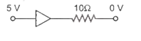
A junction diode has a resistance of 25 Ω when forward biased and 2500 Ω when reverse biased. The current in the diode, for the arrangement shown will be
In a common emitter configuration, a transistor has β = 50 and input resistance 1 kΩ. If the peak value of AC input is 0.01 V, then the peak value of collector current is
0.01 µA
0.25 µA
100 µA
500 µA


