 Multiple Choice Questions
The Input resistance of silicon transistor 100Ω. Base current is changed by 40 uA which results in a change in collector current by 2 mA. This transistor is used as common-emitter amplifier with a load resistance of 4 kΩ. The voltage gain of the amplifier is
2000
3000
4000
4000
To get an output Y = 1 in given circuit which of the following input will be correct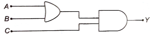
|
A |
B |
C |
|
1 |
0 |
0 |
|
A |
B |
C |
|
1 |
0 |
1 |
|
A |
B |
C |
|
1 |
1 |
0 |
|
A |
B |
C |
|
1 |
1 |
0 |
In a CE transistor amplifier, the audio signal voltage across the collector resistance of 2kΩ is 2V. If the base resistance is 1kΩ and the current amplification of the transistor is 100, the input signal voltage is
0.1 V
1.0 V
1 mV
1 mV
C and si both have a same lattice structure, having 4 bonding electrons in each. However, C is insulator whereas Si is an intrinsic semiconductor. This is because
in the case of C, the valence band is not completely filled at absolute zero temperature
in a case C, the conduction band is partly filled even at absolute zero temperature
the four bonding electrons in the case of C lie in the second orbit, whereas in case of Si they lie in the third
the four bonding electrons in the case of C lie in the second orbit, whereas in case of Si they lie in the third
The figure shows a logic circuit with two inputs A and B and the output C. The voltage waveforms across A, B and C are as given. The logic circuit gate is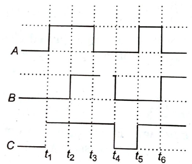
OR Gate
NOR Gate
AND Gate
AND Gate
Transfer characteristic [output voltage (Vo) vs input voltage (Vi)] for a base biased transistor in CE configuration is as shown in the figure. For using transistor as a switch, it is used
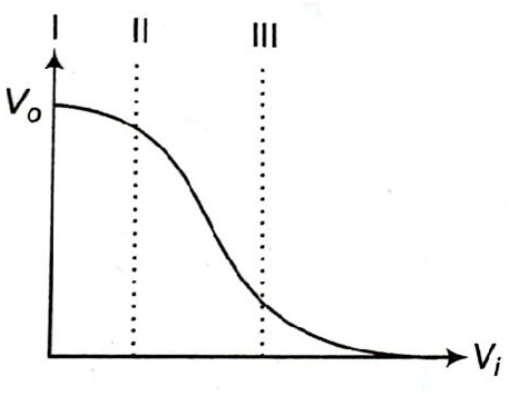
in region III
both in region (I) and (III)
in region (II)
in region (II)
B.
both in region (I) and (III)
For using a transistor as a switch, it is used in cut-off state and saturation state only.
Two ideal diodes are connected to a battery as shown in the circuit. The current supplied by the battery is
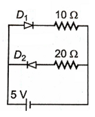
0.75 A
zero
0.25
0.25
The given graph represents V-I characteristic for a semiconductor device. Which of the following statement is correct?
It is V-I characteristic for solar cell where point A represents open circuit voltage and point B short circuit current.
It is for a solar cell and points A and B represent open circuit voltage and current, respectively.
It is for a photodiode and points A and B represent open circuit voltage and current, respectively.
It is for a photodiode and points A and B represent open circuit voltage and current, respectively.
The barrier potential of a p-n junction diode depends on:
i) type of semiconductor material
ii) amount of doping
iii) temperature
Which one of the following is correct?
(i) and (ii) only
(ii) only
(ii) and (iii) only
(ii) and (iii) only


 Switch


