Multiple Choice Questions
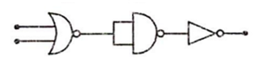
Which logic gate is represented by the following, combination of logic gates in figure?
OR
NAND
AND
NOR
C.
AND
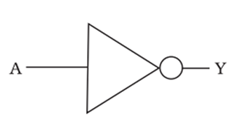
NOT gate:- This is the most basic gate. with one input and one output. It produces a ' 1 ' output if the input is ' 0 ' and vice-versa. That it produces an inverted inversion of the input at its output.
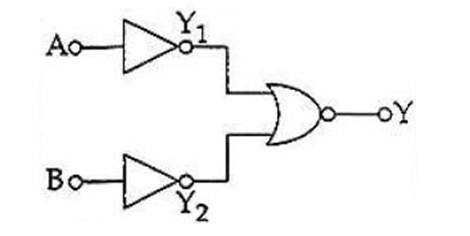
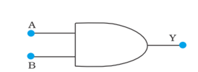
AND gate:- An AND gate has two or more inputs and one output. The output Y of AND gate is 1 only when input A and input B are both 1. The logic symbol and truth table for this gates as shown below.
| A | B | Y1 | Y2 | Y = |
| 0 | 0 | 1 | 1 | 0 |
| 0 | 1 | 1 | 0 | 0 |
| 1 | 0 | 0 | 1 | 0 |
| 1 | 1 | 0 | 0 | 1 |
According to the truth table
Y = A · B
the given combination of logic gates represents AND gate.
Which of the given statements about transistor is not true?
Emitter is heavily doped.
Base is thin.
Base is lightly doped.
Collector region is smaller comparative to emitter in size.
Assertion: The resistance of a junction of a spoiled transistor is low when forward biased or reverse biased.
Reason: The resistance of a junction of a transistor in working order is high always.
If both assertion and reason are true and reason is the correct explanation of assertion.
If both assertion and reason are true but reason is not the correct explanation of assertion.
If assertion is true but reason is false.
If both assertion and reason are false.n
In an intrinsic semiconductor band gap is 1.2 eV then ratio of number of charge carriers at 600 K and 300 K is
104
107
105
103
Assertion: Electric appliances with metallic body. e.g., heaters, presses etc., have three pin connections, whereas an electric bulb has a two pin connection.
Reason: Three pin connections reduce heating of connecting cables.
If both assertion and reason are true and reason is the correct explanation of assertion.
If both assertion and reason are true but reason is not the correct explanation of assertion.
If assertion is true but reason is false.
If both assertion and reason are false.
Which of the following current must be zero in an unbiased PN junction diode?
Current due to majority charge carriers (both electrons and holes).
Current due to minority charge carriers (both electrons and holes).
Current due to majority and minority charge carriers
Current due to majority and minority charge carriers (only holes).
For a common-emitter transistor, input current is 5A, ( β = 100 circuit is operated at load resistance of 10 kΩ, then voltage across collector emitter will be
5 V
10 V
12.5 V
7.5 V
Direction of electric field in P-N junction diode is
from P-side to N-side
From N-side to P-side
randomly oriented
electric field does not exist
Assertion: Photodiode and photovoltaic cell are based on the same principle.
Reason: Both use same method of operations to work.
If both assertion and reason are true and reason is the correct explanation of assertion.
If both assertion and reason are true but reason is not correct explanation of assertion.
If assertion is true but reason is false.
If both assertion and reason are false.


 Switch