Multiple Choice Questions
The following figure shows a logic gate circuit with two inputs A and B the output Y. The voltage waveforms of A, B and Y are as given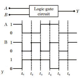
The logic gate is
NOR gate
OR Gate
AND gate
AND gate
A p-n photodiode is fabricated from a semiconductor with a band gap of 2.5 eV. It ca detect a signal of wavelength
6000 Ao
4000 nm
6000 nm
6000 nm
If a diamagnetic substance is brought near the north or the south pole of a bar magnet, it is
repelled by both the poles
repelled by the north pole and attracted by the south pole
attracted by the north pole and repelled by the south pole
attracted by the north pole and repelled by the south pole
The symbolic representation of four logic gates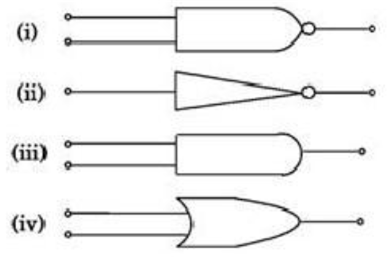
The logic symbols for OR, NOT and NAND gates are respectively
(iii), (iv), (ii)
(iv), (i), (iii)
(iv), (ii), (i)
(iv), (ii), (i)
A transistor is operated in common-emitter configuration at Vc = 2 volts such that a change in the base current from 100 μ A to 200 μ A produces a change in the collector current from 5 mA to 10 mA. The current gain is
75
100
150
150
A p-n photodiode is made of a material with a band gap of 2.0 eV. The minimum frequency of the radiation that can be absorbed by the material is nearly
10 x 1014 Hz
5 x 10¹⁴ Hz
1 x 10¹⁴ Hz
1 x 10¹⁴ Hz
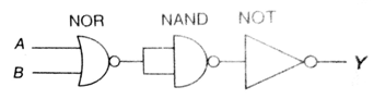
In the following circuit the output Y for all possible input A and B is expressed by the truth table:![]()
| A | B | Y |
| 0 | 0 | 0 |
| 0 | 1 | 0 |
| 1 | 0 | 0 |
| 1 | 1 | 1 |
| A | B | Y |
| 0 | 0 | 1 |
| 0 | 1 | 1 |
| 1 | 0 | 1 |
| 1 | 1 | 0 |
| A | B | Y |
| 0 | 0 | 1 |
| 0 | 1 | 1 |
| 1 | 0 | 1 |
| 1 | 1 | 0 |
| A | B | Y |
| 0 | 0 | 1 |
| 0 | 1 | 1 |
| 1 | 0 | 1 |
| 1 | 1 | 0 |
In the energy band diagram of a material shown below, the open circles and filled circles denote holes and electrons respectively. The material is a/an,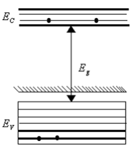
p-type semiconductor
insulator
metal
metal
A transistor is operated in common emitter configuration at constant collector voltage Vc = 1.5 V such that a change in the base current from 100 µA to 150 µA produces a change in the collector current from 5 mA to 10 mA. The current gain (β) is
67
75
100
100