Advertisement

Explain, with the help of a circuit diagram, how the thickness of depletion layer in a p-n junction diode changes when it is forward biased. In the following circuit which one of the two diodes is forward biased and which is reverse biased? 


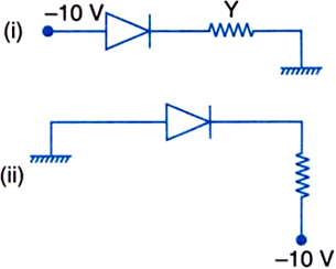
(i) In this case, the p-side is at -10 V, whereas the n-side is at 0 V. Vp < VN, hence, the diode is reverse biased.
(ii) In this case, the p-side is at 0 V, whereas the n-side is at -10 V. Vp > VN, hence, the diode is forward biased.
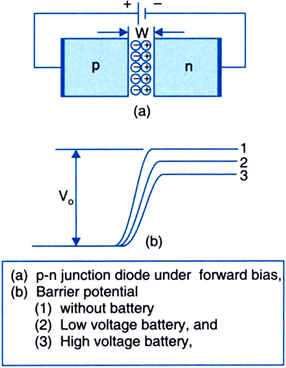
When applied voltage is such that n-side is negative and p-side is positive, the applied voltage is opposite to the barrier potential. Hence, the effective barrier potential becomes VB-V, and the energy barrier across the junction decreases. Thus, the junction width decreases.
(i) p-n junction is forward biased.
(ii) p-n junction is reverse biased.

(i) In this case, the p-side is at -10 V, whereas the n-side is at 0
                       

349 Views

Advertisement

Semiconductor Electronics: Materials, Devices and Simple Circuits

Hope you found this question and answer to be good. Find many more questions on Semiconductor Electronics: Materials, Devices and Simple Circuits with answers for your assignments and practice.

Physics Part II

Browse through more topics from Physics Part II for questions and snapshot.