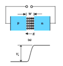
(i) Explain with the help of a diagram the formation of depletion region and barrier potential in a p-n junction.
(ii) Draw the circuit diagram of a half wave rectifier and explain its working.
i)
In a p-n junction, a p-type and an n-type material are joined together. P-type has a higher concentration of holes and n-type has a higher concentration of electrons. Hence, there is a concentration gradient between the p-type and n-type materials. Therefore, holes drift from p-side to n-side by the process of diffusion due to concentration gradient. In a similar manner, electrons move from n-side to p-side.
As a result of the movement of holes from p-side, they leave ionised spaces (negative charge) on p-side near the junction. Similarly, a positive space charge region is formed on the n-side due to the diffusion of electrons from n-side. The two space charge regions on either side of the junction is called as
depletion region.
A potential difference is developed across the junction of two regions, which is known as the
barrier potential. The reverse polarity of this potential opposes further flow of carriers.
ii)
Half wave rectifier:
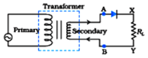 Working
: When an alternating voltage is applied across a diode in series with a load, a pulsating voltage will appear across the load only during that half cycle on the AC input during which the diode is forward biased.
In the positive half cycle of AC input, a current flows through load resistance R
L and we get the output voltage.
In the negative half cycle, there is no output. Therefore, the output voltage is restricted to only one direction and is said to be rectified.
3995 Views