Draw V – I characteristics of a p–n junction diode. Answer the following questions, giving reasons:
(i) Why is the current under reverse bias almost independent of the applied potential up to a critical voltage?
(ii) Why does the reverse current show a sudden increase at the critical voltage?
Name any semiconductor device which operates under the reverse bias in the breakdown region. 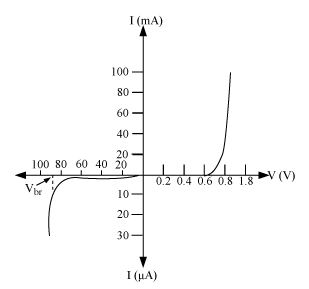
V-I characteristics of p-n junction diode are as shown on the right side:
i) The current of order in reverse biasing is due to the drifting of minority charge carriers from one region to another through the junction. A small amount of applied voltage is sufficient to sweep the minority charge carriers through the junction. So reverse current is almost independent of critical voltage.
ii) During the critical voltage or most commonly called breakdown voltage, enormous covalent bonds break. As a result, large number of charge carriers increase. Therefore, current increases at critical voltage.
Zener diode operates under the reverse bias in the breakdown region.


