 Multiple Choice Questions
Which one of the following statement is false?
Pure Si doped with trivalent impurities given a p- type semiconductor
Majority carriers in a p- type semiconductor are holes
Minority carriers in a p- type semiconductor are electron
Minority carriers in a p- type semiconductor are electron
The device that can act as a complete electronic circuit is
Junction diode
Integrated circuit
Junction transistor
Junction transistor
A common emitter amplifier has a voltage gain of 50, an input impedance of 100 Ω and an output impedance of 200 Ω. The power gain the amplifier is
500
1000
1250
1250
To get an output Y = 1 from the circuit shown below, the input must be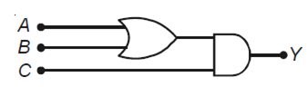
|
A |
B |
C |
|
0 |
1 |
0 |
|
A |
B |
C |
|
0 |
0 |
1 |
|
A
|
B
|
C
|
|
1
|
0
|
1
|
|
A
|
B
|
C
|
|
1
|
0
|
1
|
For transistor action
A) Base, emitter and collector regions should have similar size and doping concentrations.
B) The base region must be very thin and lightly doped.
C) The emitter-base junction is forward biased and base -collector junction is reverse biased
D) Both the emitter-base junction as well as the base-collector junction are forward biased.
(D) and (A)
(A) and (B)
(B) and (C)
(B) and (C)
The following figure shows a logic gate circuit with two inputs A and B the output Y. The voltage waveforms of A, B and Y are as given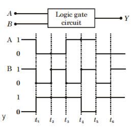
The logic gate is
NOR gate
OR Gate
AND gate
AND gate
A p-n photodiode is fabricated from a semiconductor with a band gap of 2.5 eV. It ca detect a signal of wavelength
6000 Ao
4000 nm
6000 nm
6000 nm
If a diamagnetic substance is brought near the north or the south pole of a bar magnet, it is
repelled by both the poles
repelled by the north pole and attracted by the south pole
attracted by the north pole and repelled by the south pole
attracted by the north pole and repelled by the south pole
The symbolic representation of four logic gates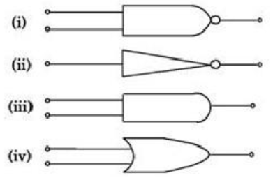
The logic symbols for OR, NOT and NAND gates are respectively
(iii), (iv), (ii)
(iv), (i), (iii)
(iv), (ii), (i)
(iv), (ii), (i)
A transistor is operated in common-emitter configuration at Vc = 2 volts such that a change in the base current from 100 μ A to 200 μ A produces a change in the collector current from 5 mA to 10 mA. The current gain is
75
100
150
150


