Multiple Choice Questions
A p-n photodiode is made of a material with a band gap of 2.0 eV. The minimum frequency of the radiation that can be absorbed by the material is nearly
10 x 1014 Hz
5 x 10¹⁴ Hz
1 x 10¹⁴ Hz
1 x 10¹⁴ Hz
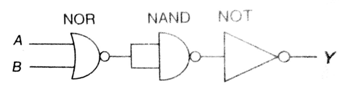
In the following circuit the output Y for all possible input A and B is expressed by the truth table:![]()
| A | B | Y |
| 0 | 0 | 0 |
| 0 | 1 | 0 |
| 1 | 0 | 0 |
| 1 | 1 | 1 |
| A | B | Y |
| 0 | 0 | 1 |
| 0 | 1 | 1 |
| 1 | 0 | 1 |
| 1 | 1 | 0 |
| A | B | Y |
| 0 | 0 | 1 |
| 0 | 1 | 1 |
| 1 | 0 | 1 |
| 1 | 1 | 0 |
| A | B | Y |
| 0 | 0 | 1 |
| 0 | 1 | 1 |
| 1 | 0 | 1 |
| 1 | 1 | 0 |
In the energy band diagram of a material shown below, the open circles and filled circles denote holes and electrons respectively. The material is a/an,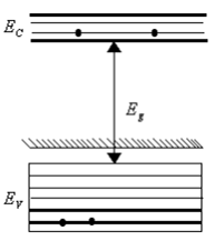
p-type semiconductor
insulator
metal
metal
A transistor is operated in common emitter configuration at constant collector voltage Vc = 1.5 V such that a change in the base current from 100 µA to 150 µA produces a change in the collector current from 5 mA to 10 mA. The current gain (β) is
67
75
100
100
The following figure shows a logic gate circuit with two inputs A and B and the output C. The voltage waveforms of A, B and C are as shown below:
The logic curcuit gate is
AND gate
NAND gate
NOR gate
NOR gate
In a common emitter transistor amplifier, the audio signal voltage across the collector is 3 V. The resistance of collector is 3 kΩ. If current gain is 100 and the base resistance is 2 kΩ, the voltage and power gain of the amplifier is
200 and 1000
15 and 200
150 and 15000
150 and 15000