CBSE Multiple Choice Questions
In forward biasing of the p - n junction
the positive terminal of the battery is connected to n - side and the depletion region becomes thin
the positive terminal of the battery is connected to n- side and the depletion region becomes thick
the positive terminal of the battery is connected to p - side and the depletion region become thin
the positive terminal of the battery is connected to p - side and the depletion region become thin
Two ideal diodes are connected to a battery as shown in the circuit. The current supplied by the battery is
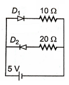
0.75 A
zero
0.25
0.25
The barrier potential of a p-n junction diode depends on:
i) type of semiconductor material
ii) amount of doping
iii) temperature
Which one of the following is correct?
(i) and (ii) only
(ii) only
(ii) and (iii) only
(ii) and (iii) only
Transfer characteristic [output voltage (Vo) vs input voltage (Vi)] for a base biased transistor in CE configuration is as shown in the figure. For using transistor as a switch, it is used
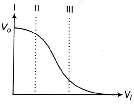
in region III
both in region (I) and (III)
in region (II)
in region (II)
The given graph represents V-I characteristic for a semiconductor device. Which of the following statement is correct?
It is V-I characteristic for solar cell where point A represents open circuit voltage and point B short circuit current.
It is for a solar cell and points A and B represent open circuit voltage and current, respectively.
It is for a photodiode and points A and B represent open circuit voltage and current, respectively.
It is for a photodiode and points A and B represent open circuit voltage and current, respectively.
If a small amount of antimony is added to germanium crystal
the antimony becomes an acceptor atom
there will be more free electrons than holes in the semiconductor
its resistance is increased
its resistance is increased
The output (X) of the logic circuit shown in a figure will be.![]()


X = A. B
X = A. B
In an n-type semiconductor, which of the following statement is true?
Electrons are majority carriers and trivalent atoms are dopants
Electrons are minority carriers and pentavalent atoms are dopants
Holes are minority carriers and pentavalent atoms are dopants
Holes are minority carriers and pentavalent atoms are dopants
Symbolic representation of four logic gates are shown as,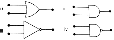
Pick out which ones are for AND, NAND and NOT gates, respectively.
(iii), (ii) and (i)
(iii), (ii) and (i)
(ii), (iv), and (iii)
(ii), (iv), and (iii)
In a common emitter (CE) amplifier having a voltage gainG, the transistor used has transconductance 0.03 mho and current gain 25. If the above transistor is replaced with another one with transconductance 0.02 mho and current gain 20, the voltage gain will
2/3 G
1.5 G
1/3 G
1/3 G